

GPT-6 Astra and the Future of PCB Design: Speed Up or Replace Engineers?
How far can GPT-6 Astra go in KiCad? An independent look at the demo, EEBench, open-source tools, and why routing a board is not the same as making it production-ready.
Share
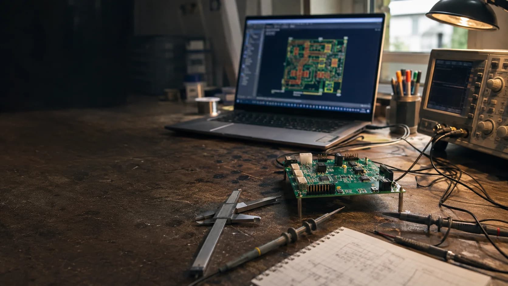
A short video of GPT-6 Astra operating on a PCB inside KiCad was enough to get the hardware community talking. The model takes an electronic design, places components, routes traces, and produces a board that looks surprisingly complete. The natural question is: if AI can already handle the visible part of PCB work, what is left for a PCB engineer?
My current answer is straightforward: AI will speed up PCB design, but it does not replace the engineer responsible for making the board work and manufacturing it reliably.
What has GPT-6 Astra actually demonstrated?
OpenAI presents GPT-6 Astra as a model with computer-use and professional-work capabilities. Its electrical-engineering examples include operating design software such as KiCad. The model documentation also lists computer use, file search, code interpreter, and hosted shell as supported capabilities (OpenAI, model documentation).
The important part is not only that the model “knows KiCad.” It can observe application state, perform multiple actions, and turn a technical request into an artifact that can continue through a toolchain. For repetitive work such as constraint-based placement, net connections, geometric fixes, or release-file generation, that integration matters.
But a demo is still a demo. A short video shows that a model can complete a prepared workflow under specific conditions. It does not prove that every PCB can be sent straight to a factory.
How should we read the EEBench number?
EEBench is an electrical-engineering benchmark built by the Atopile team. Its current leaderboard shows GPT-6 Astra at 69.3 ± 10.7%, with an average cost of about $0.83 per task and a time of about 1 minute 46 seconds. That is interesting, but it is a score on a defined task set, not a real-world “percentage of boards that work.”
I would also include the date whenever quoting that number. The first EEBench blog post said they did not yet have an Astra result, while the leaderboard was later updated with one. Benchmarks change with time, harness, and task set; a leaderboard row should not become a production promise.
EEBench makes another useful distinction: it runs tasks in Atopile's declarative environment, where an agent can edit a design, build it, simulate it, and inspect failures. That is different from asking an AI to click around a GUI. Atopile on GitHub describes a code-based electronics toolchain with validation and KiCad-compatible layout; the EEBench methodology also documents its provenance and limits.
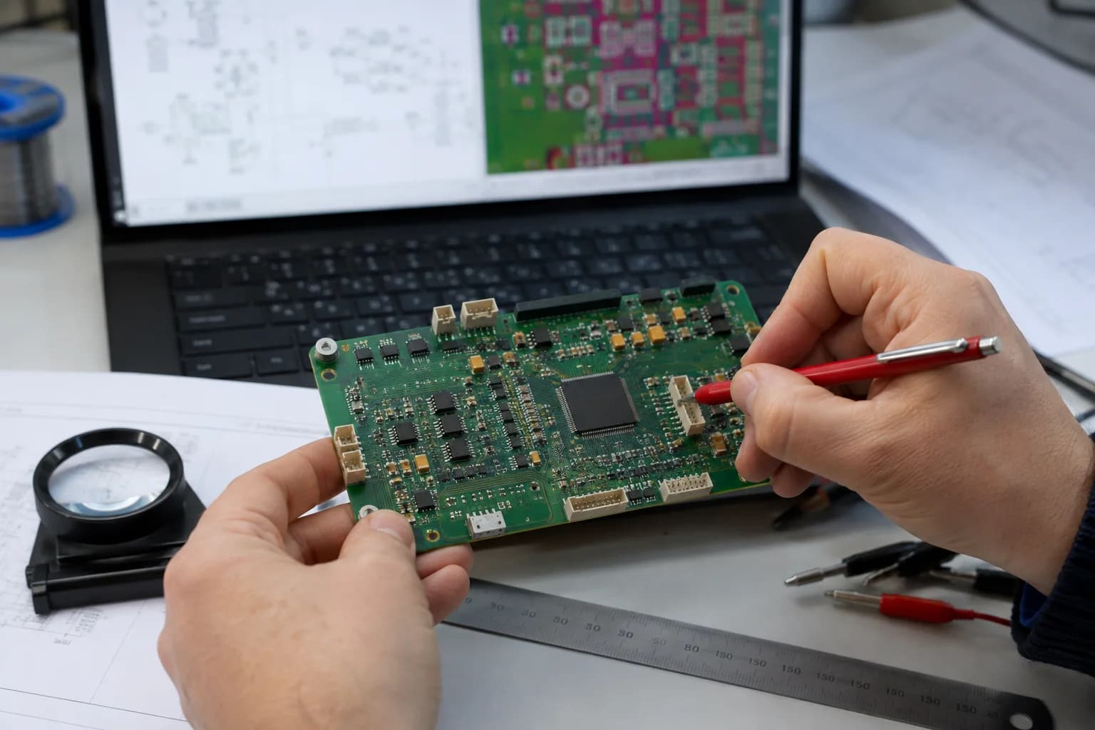
AI can produce a layout worth inspecting, but schematic, datasheet, and constraint review still needs system understanding.
A routed board is not necessarily a working board
A layout can look excellent and still fail in important ways:
- the footprint does not match the real package, or the pin numbering is wrong;
- decoupling is too far from the power pins, or the return path is poor;
- power, peak current, or thermal limits are not respected;
- USB, crystal, RF, or differential pairs violate their real constraints;
- connectors and mounting holes do not fit the enclosure;
- the BOM contains unavailable parts or packages the assembler cannot place;
- ERC/DRC is clean while the schematic still expresses the wrong system intent.
ERC checks part of the schematic's electrical rules. DRC checks many geometric and layout rules. Both are necessary, but neither is complete evidence for signal integrity, power integrity, EMC, thermal behavior, mechanics, or firmware bring-up.
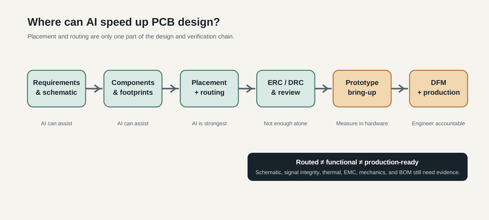
Placement and routing are only two middle steps in a much longer validation chain.
Where AI can create real speed-ups
AI is most useful when the input and output are reasonably well defined:
- Turn a clear requirement into a block schematic or a familiar circuit template.
- Find alternates, compare parametric constraints, and create a draft BOM.
- Generate symbols, footprints, net labels, test points, or configuration files.
- Place components and route less-sensitive nets after constraints are defined.
- Run ERC/DRC, group findings, and suggest changes.
- Generate Gerbers, drill files, pick-and-place data, BOMs, and release documents.
In this role, AI looks like an extremely fast junior engineer for manipulation-heavy work. The clearer the input — layer stackup, trace width, clearance, keepout, placement constraints, preferred parts, and rules — the easier the output is to review.
What should not be fully delegated yet
I would not let an AI make the final call on:
- power topology, compensation, and safety limits;
- pinout, absolute maximum ratings, and thermal conditions;
- RF, antenna, high-speed, and sensitive mixed-signal layout;
- creepage and clearance for high voltage;
- enclosure, connector, mounting, and service decisions;
- signing the release package sent to a manufacturer.
This is not because AI is “not smart enough.” These decisions depend on context that may not exist in the schematic: the real enclosure, real cables, real users, real factory capabilities, real component revisions, and failures from the previous board revision.
What open-source Git projects are showing us
If I wanted to try AI-assisted EDA today, I would begin with projects whose source and outputs can be inspected:
- Atopile: code-based circuit design with reusable modules, constraints, and validation, followed by KiCad-compatible layout.
- kicad-mcp: an MCP server for an agent to operate on KiCad schematics and PCBs.
- kicad-mcp-server: an agent-to-KiCad connection through the IPC API.
- kicad-action: automated ERC/DRC and production-file generation in GitHub Actions.
- KiCadAI: a structured toolkit for KiCad project generation, validation, and pin-map checks.
What I like about these projects is that they show AI should not stand alone. The agent needs a parser, compiler, simulator, ERC/DRC, and CI so that every change has evidence attached to it.
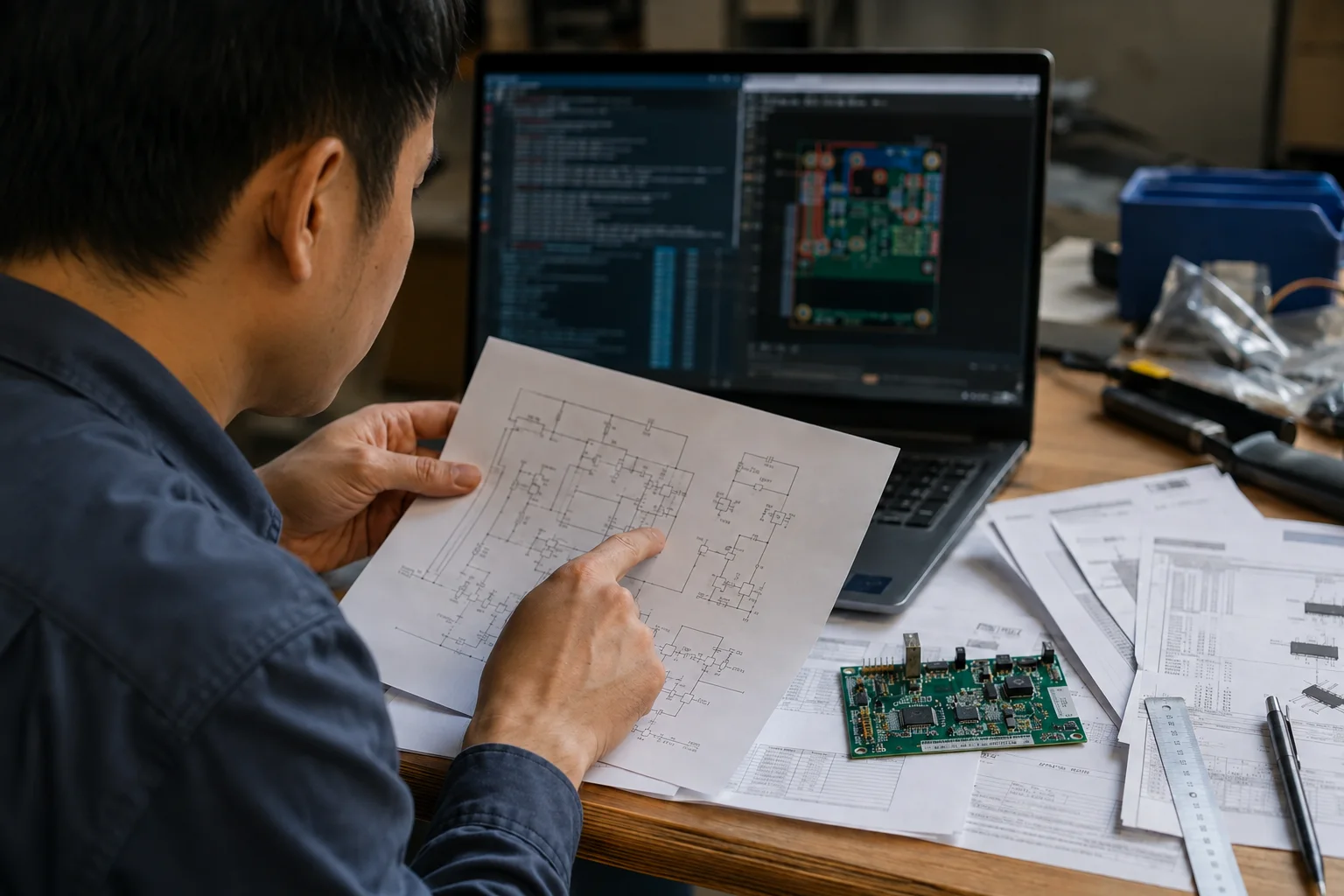
The most practical workflow today is still human-in-the-loop: AI handles repetition while engineers keep context and make the final call.
The workflow I would use on a real board
If I used GPT-6 Astra or another EDA agent on a real design, I would divide the workflow into gates.
1. Lock requirements before opening KiCad
Write down input voltage, rails, peak current, interfaces, board size, stackup, environment, target cost, and non-substitutable parts. A vague requirement only becomes professionally formatted vagueness when AI processes it.
2. Review the schematic and footprints
Check the exact component datasheet, pin 1, package, exposed pad, polarity, NC pins, and recommended circuit. Do not rely on the component name in a library alone.
3. Run ERC/DRC in a clean environment
Run KiCad or CI checks and save the reports with the commit. When an AI says “checked,” ask for the artifact: log, rule set, before/after issue count, and output file.
4. Review the layout by risk category
Check power paths, return paths, decoupling, crystal, USB, RF, high-speed pairs, thermal copper, test points, and mechanical keepouts. A checklist review is more reliable than zooming around the board and deciding that it “looks fine.”
5. Build a prototype and bring it up
Power it through a current limit; measure rails, reset, clock, buses, and temperature. Test boot failure, power loss, disconnected peripherals, reconnects, and maximum load.
6. Release to manufacturing only after that
Lock BOM availability, alternates, fab capability, assembly direction, Gerbers, drill, pick-and-place, and revision. The person signing the release should know exactly what they are signing for.
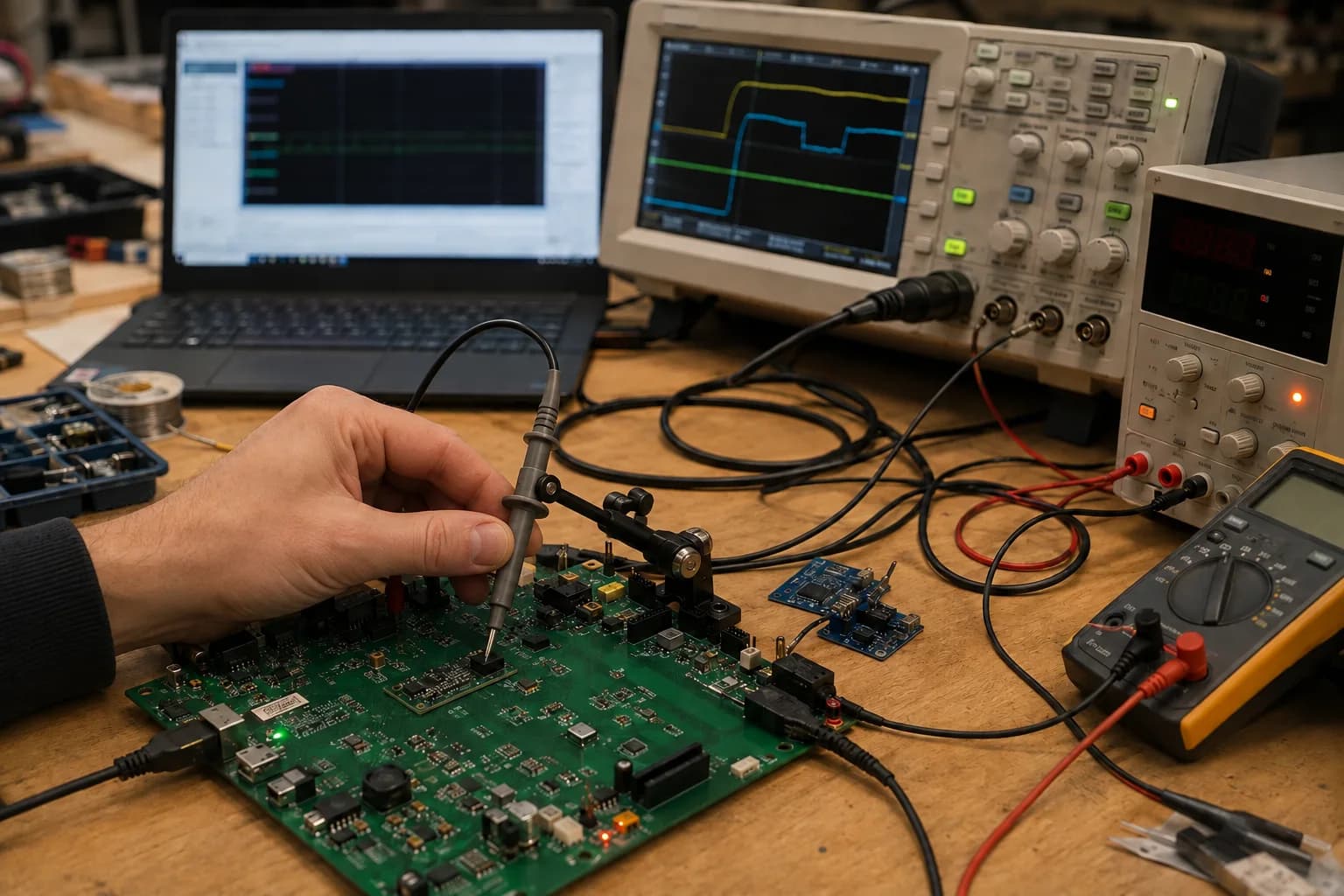
Only after powering, probing, and exercising the real board do we know whether the layout works as intended.
Will AI replace engineers or change their work?
In the near term, I expect the second outcome. AI can remove many hours of repetitive manipulation, but it makes review more important. As generating a layout becomes cheaper and faster, the valuable skills move toward:
- writing the right requirements;
- expressing constraints that can be checked;
- finding dangerous assumptions;
- reading measurement results;
- understanding the trade-offs among cost, size, yield, reliability, and time-to-market.
Engineers may spend less time dragging every trace, but they will need to get better at defining what a correct trace is and proving that it is correct.
Conclusion
GPT-6 Astra is a clear sign that AI agents are moving deeper into the EDA toolchain. The KiCad demo is notable, EEBench suggests that capability is improving, and projects such as Atopile and kicad-mcp show an open-source ecosystem forming around the workflow.
But placement and routing are geometric outputs. A production-ready PCB also needs electrical correctness, physical correctness, manufacturability, prototype testing, and a person accountable for sign-off.
So my answer is: AI will make PCB design much faster. Replace the engineer? Not yet. More likely, the engineer's role will shift from drawing the board to designing constraints, validating with evidence, and owning the final decision.
References
Share
Keep exploring
Read next
Related articles
Net Classes and Trace Width: When Should a PCB Trace Be Wider?
A practical guide to PCB net classes and trace width for small boards: signal traces, 3V3, 5V, battery paths, ground, power vias, and a pre-Gerber checklist.
PCB Ground Planes: GND Is More Than a Net Name
A practical guide to PCB ground planes, return current, GND layout mistakes, stitching vias, decoupling paths, and copper pour checks.
A Practical PCB Review Checklist Before You Send It to Fab
A practical PCB review checklist before fabrication: schematic, ERC, footprints, clearance, power, antenna, USB pairs, silkscreen, Gerbers, and BOM.