

PCB Ground Planes: GND Is More Than a Net Name
A practical guide to PCB ground planes, return current, GND layout mistakes, stitching vias, decoupling paths, and copper pour checks.
Share
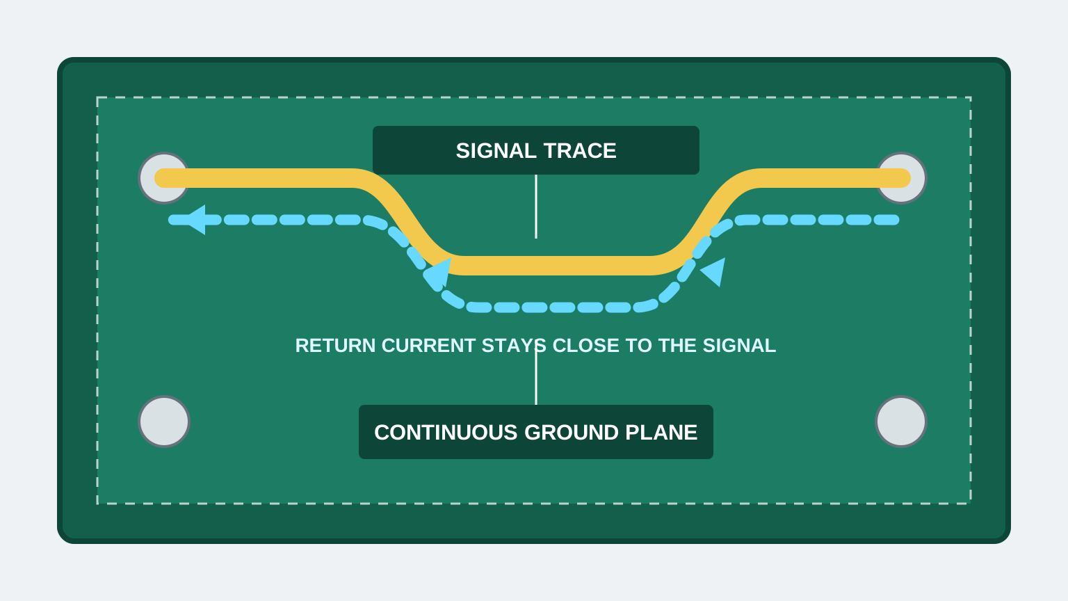
When you are new to PCB layout, it is easy to treat GND as just another net: connect every GND pin and move on. In a real board, ground is not only a schematic symbol or a 0V label. It is also the return path for current.
A ground plane handles GND as a large copper area on the PCB. Instead of routing ground through many small traces, you pour copper connected to the GND net so return current has a wider, shorter, lower-impedance path.
On small boards with an ESP32, SPI display, MEMS microphone, amplifier, buck or boost converter, or Li-ion charger, the ground layout can decide whether the circuit feels stable. A schematic can be correct while the real board still resets randomly, produces audio noise, flickers a display, weakens Wi-Fi, or gives poor sensor readings because the return path is messy.
What Is a Ground Plane?
A ground plane is a copper pour assigned to the GND net. It can live on the top layer, bottom layer, or on a dedicated internal layer in a multilayer board.
On a common 2-layer board, a practical arrangement is:
- Use the top layer for components and important signal routes.
- Keep the bottom layer as continuous GND copper as much as possible.
- If both sides have GND pours, connect them with stitching vias.
The goal is not to make the PCB look filled. The goal is to give return current a good path. Current leaves the source through the power route, passes through the load, and returns through ground. If that return path is narrow, long, or cut into pieces, the board becomes noisier and less predictable.
Why Ground Planes Matter
A good ground plane lowers the impedance of the ground path. When return current has plenty of copper available, the voltage difference between different ground points on the board stays smaller. That helps power stability, signal quality, and isolation between circuit blocks.
For medium- and higher-speed signals, ground also acts as a reference plane. An SPI line, I2S clock, or USB trace is not only about the visible signal route. Its return current tends to follow nearby on the ground plane. If that plane is split, the return current has to detour, increasing loop area and noise.
A good ground plane gives return current a short, wide path; narrow ground necks can force current to detour.
So during review, do not only ask whether the nets are connected. Ask where the return current will actually flow.
Mistake 1: Routing GND as a Thin Trace
This is common on early boards. Ground gets routed like GPIO: one narrow trace from point to point. Electrically, the schematic is connected. DRC may even be quiet. But in operation, several return currents may be forced through a long, narrow route.
Symptoms can look unrelated:
- An ESP32 resets when Wi-Fi starts or the display backlight changes.
- An amplifier produces noise that follows load activity.
- ADC or analog sensors drift.
- USB or SPI behaves intermittently.
- A multimeter shows a reasonable voltage, but the board still fails.
If there is enough room, prefer a ground plane over thin ground traces. If a ground trace is unavoidable in one section, keep it short and wide enough, especially for a high-current return path.
Mistake 2: Cutting the Plane Into Pieces
A good ground plane should be as continuous as practical. During routing, however, it is easy to cut it with signal traces, vias, keepouts, mechanical slots, mounting holes, or no-copper regions.
When the plane is cut, return current cannot follow the shortest path. It has to route around the split or squeeze through a narrow neck. With fast display SPI, I2S clocks, USB, or switching-regulator current pulses, that detour can increase noise and reduce stability.
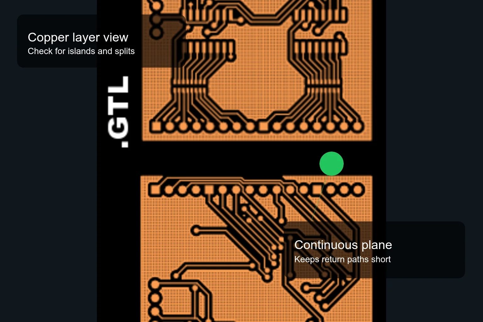
After pouring copper, inspect the layer view for islands, splits and plane areas that are no longer continuous.
After pouring copper, inspect GND intentionally:
- Are there isolated GND islands?
- Does any route cut across the plane under a fast signal?
- Is there a narrow ground neck between two large copper areas?
- Is a copper area visually large but not actually connected to the main
GNDnet?
Do not review only with all layers shown at once. Highlight GND and look at the copper layer by itself so you can see the real return path.
Mistake 3: Not Connecting GND Between Layers
If a board has GND pours on both top and bottom, they need vias between them. Without enough GND vias, the two copper areas may only connect through a few distant or narrow points. In that case they do not behave like one shared plane.
Stitching vias connect GND areas between layers. You do not need to place them mechanically everywhere, but they should appear where they matter:
- Near GND pins of regulators, ESP32 modules, amplifiers, and power connectors.
- Near decoupling capacitors so noise current has a short path into the plane.
- Along board edges or near fast signals when you need a continuous reference.
- Near signal layer changes, so return current can change layers too.
A well-placed GND via is often worth more than many random ones.
Mistake 4: Letting Power Return Current Cross Sensitive Areas
Not every ground current is equally quiet. Motor, speaker, power LED, charger, and switching-regulator currents are usually much noisier than the return current from a MEMS microphone, analog sensor, or ADC input.
If noisy current crosses a sensitive area, it can couple into small signals:
- Audio picks up buzz or hiss.
- A microphone has a noisy floor.
- ADC readings jump when LEDs or motors switch.
- An ESP32 resets when a charger or power load changes state.
The answer is not always to split ground into separate islands. On small boards, splitting ground poorly can make the return path worse. A more practical approach is block placement: keep power, charging, motors, and LEDs close to their return path, and avoid routing their return current through microphone, analog, ADC, or antenna regions.
Mistake 5: Decoupling Capacitors With a Long Ground Path
A decoupling capacitor only works well when its current loop is small. Placing a 100nF capacitor near an IC on the schematic is not enough. In layout, the capacitor power pin should be near the IC power pin, and the capacitor ground pin should connect to the ground plane with a very short path.
If the capacitor is physically near the IC but its ground side takes a long path to reach the plane, its effectiveness drops. For ESP32 modules, regulators, MEMS microphones, amplifiers, and interface ICs, prioritize:
- Put the capacitor close to the power pin it supports.
- Give the capacitor ground pin a nearby via into the ground plane.
- Avoid sending the capacitor return through a narrow neck or long detour.
- Place larger bulk capacitors close to the power entry point or high-current load.
For the other half of this topic, the article on choosing capacitors for electronics pairs well with this one.
Mistake 6: Pouring GND but Not Checking It
After clicking copper pour, do not assume a filled-looking board is correct. Some problems only show up when you highlight a net or run DRC:
- A GND island is not connected to the main ground.
- A GND pad does not connect because of clearance or thermal relief settings.
- A copper area belongs to another net, not
GND. - A GND via does not connect because of layer or rule configuration.
- A keepout slot divides the plane into two regions.
Before exporting Gerbers, highlight the GND net, run DRC, and open the exported files in a Gerber viewer. This also belongs in a broader PCB review checklist before fabrication.
Ground checks pair well with net-class checks. If the board also has battery, USB, or high-current paths, review them with the PCB net class and trace width guide before locking the layout.
A Quick GND Checklist
Before sending a board out, I like to ask:
- Is GND handled with a useful plane or mostly with small traces?
- Is the ground plane cut by traces, keepouts, or mounting holes?
- Are there any GND islands disconnected from the main net?
- Do top and bottom GND pours have stitching vias where they matter?
- Does high-current return flow through microphone, audio, ADC, or antenna areas?
- Do decoupling capacitors have short ground paths into the plane?
- Are the ESP32 power and ground paths wide enough and close to their capacitors?
- Do DRC and the Gerber viewer confirm that GND is connected correctly?
This checklist is not a substitute for layout experience, but it catches many problems before fabrication.
Conclusion
A ground plane looks simple, but it can decide whether a board is stable. GND is not a decorative connection. It is the return path for the entire circuit.
When you are starting, keep the rules practical: use a ground plane instead of narrow GND traces when possible, keep the plane continuous, place GND vias where return current needs them, avoid sending power return through sensitive regions, and always inspect GND after pouring copper.
For ESP32 boards, displays, microphones, speakers, battery supplies, and Li-ion chargers, a better ground layout often makes the circuit behave much more calmly. Hardware debugging is still hard, but at least you will avoid chasing noise problems caused by a return path that had nowhere good to go.
References
These sources are useful background material for checking terminology, limits, and engineering recommendations before applying the notes to a real prototype.
- Analog Devices: Staying Well Grounded
- Analog Devices FAQ: should analog and digital ground planes be separated?
- Espressif ESP32-S3 Hardware Design Guidelines
Image provenance
The ground-plane/return-path diagram and copper-layer inspection visual were created specifically for Nastrotek to explain the principles in this article; they are not photographs copied from an external PCB project or product.
Share
Keep exploring
Read next
Related articles
Net Classes and Trace Width: When Should a PCB Trace Be Wider?
A practical guide to PCB net classes and trace width for small boards: signal traces, 3V3, 5V, battery paths, ground, power vias, and a pre-Gerber checklist.
Choosing Capacitors for Electronics: Simple Part, Easy Mistake
A beginner guide to choosing capacitors for circuits: capacitance, voltage rating, decoupling, ceramic types, DC bias, and ESP32 values.
A Practical PCB Review Checklist Before You Send It to Fab
A practical PCB review checklist before fabrication: schematic, ERC, footprints, clearance, power, antenna, USB pairs, silkscreen, Gerbers, and BOM.