

Net Classes and Trace Width: When Should a PCB Trace Be Wider?
A practical guide to PCB net classes and trace width for small boards: signal traces, 3V3, 5V, battery paths, ground, power vias, and a pre-Gerber checklist.
Share
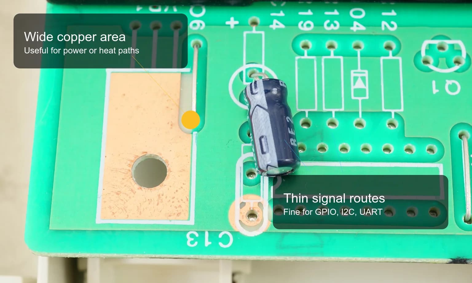
When you first start routing PCBs, it is tempting to treat every connection the same way: the schematic has a net, the trace fits on the board, DRC is quiet, so the job must be done. Real boards are less forgiving. A GPIO trace and the main 3.3V rail feeding an ESP32 should not be routed with the same assumptions.
Net classes help you group nets by design rules. Trace width is the physical width of the copper route on the PCB. Together, they turn routing intent into something your PCB tool can check: ordinary signals can stay small, power paths get more copper, and special nets such as USB do not get mixed into the default bucket.
What Is a Net Class?
In a schematic, each electrical connection belongs to a net: 3V3, GND, VBAT, I2C_SDA, SPI_MOSI, USB_D+, USB_D-, and so on.
A net class is a group of nets that share the same design rules. Instead of tuning every route by hand, you create a few meaningful groups and assign rules to each one:
Signal: GPIO, I2C, SPI, UART, and normal control signals.Power_3V3: the 3.3V rail for the MCU, sensors, and small displays.Power_5V: USB 5V, VBUS, and regulator input paths.Battery: VBAT, BAT+, Li-Po battery paths, and charger connections.GND: important ground connections, usually better handled as a plane than as thin traces.USB:USB_D+andUSB_D-.High_Current: motors, power LEDs, speakers, heaters, chargers, or any load that pulls meaningful current.
The useful part is not the naming itself. The useful part is that your intent becomes checkable. If VBAT accidentally routes with the same thin width as a GPIO, your rules can catch it before fabrication.
Why Trace Width Matters
A PCB trace is still a conductor. It is just a very flat one. A narrow, long trace has more resistance. When current flows through it, that resistance can cause voltage drop, heat, or unstable behavior.
On a small ESP32 board, sensor board, SPI display module, audio board, or battery-powered prototype, not every trace needs to be large. But the main power paths deserve more attention than ordinary signals.
A simple starting mental model:
- GPIO, I2C, and UART usually carry very little current.
- SPI for a display may need clean routing, but it is usually not a high-current path.
- The main
3V3rail for an ESP32 should be wider than a signal trace, because Wi-Fi and Bluetooth can create current peaks. 5Vfrom USB-C andVBATfrom a battery should be wider when board space allows.- Speaker, motor, charger, and power LED paths should not be routed like tiny logic traces.
If you have room, making power traces wider is usually a calm choice. It does not make the design fancy; it simply gives current an easier path.
The same board can use a wide copper area for power or heat paths while keeping ordinary signal traces much narrower.
Signal Traces and Power Traces Are Different
Signal traces mostly carry logic levels. Their current is usually tiny, so the main goals are clean routing, reasonable spacing, short loops, and keeping sensitive signals away from noisy areas.
Power traces feed actual blocks of the circuit. If the power path is too narrow or takes a long route around the board, the voltage at the load can dip when the ESP32 turns on Wi-Fi, a display brightens, an amplifier plays audio, or a charger enters a higher-current state.
When routing, I usually prioritize:
- Keep main power paths short and wide.
- Use a ground plane when possible instead of many small ground traces.
- Place decoupling capacitors close to the IC power pins, with a short return path to ground.
- Avoid sending the main rail on a long tour around the board before it reaches the load.
- Keep noisy power paths away from microphones, analog audio, antennas, and small measurement signals.
This is also why a practical PCB review checklist should include power and ground return checks, not just footprint checks.
Practical Trace Widths for Small ESP32 Boards
There is no single trace-width table that works for every PCB. The right value depends on current, trace length, copper weight, whether the trace is on an outer or inner layer, allowed temperature rise, and your manufacturer’s capabilities.
Still, for small ESP32-style boards with moderate current and common 1 oz copper, these numbers are useful starting points:
| Route group | Practical starting point |
|---|---|
| Ordinary signal | 0.15-0.20 mm |
| I2C, UART, GPIO | 0.15-0.25 mm |
| SPI for a small display | 0.20-0.30 mm |
| Main 3.3V rail | 0.40-0.80 mm |
| 5V or VBAT path | 0.60-1.00 mm if space allows |
| Speaker, motor, power LED, charger path | calculate from real current, often wider |
| GND | prefer a copper plane and enough stitching vias |
This table is not a replacement for a current calculator or a datasheet. It is a starting point that avoids one very common beginner mistake: routing every net with the same narrow default width.
When Should a Trace Be Wider?
Make a trace wider when it carries meaningful current, runs a long distance, or directly affects the stability of the board.
Common examples:
- The path from USB-C into the power section.
- The path from a Li-Po battery into protection, charging, or regulation.
- The charger output path back to the battery.
- The
3V3rail feeding the ESP32, display, sensors, and amplifier. - Routes feeding speakers, motors, power LEDs, or switched loads.
- Main ground return paths between power blocks and loads.
- Paths with high peak current, even if the average current looks modest.
A subtle trap is looking only at average current. An ESP32 may not draw a huge average current, but short Wi-Fi transmit peaks can expose a weak 3.3V route. A multimeter may miss the dip, while the board still resets.
Vias Can Become Bottlenecks Too
A via is not an unlimited conductor. It has resistance, inductance, and current limits. If a wide power trace reaches a single tiny via and all current has to squeeze through that via to another layer, the via can become the weak point.
For ordinary signals, a small via is usually fine. For VBAT, 5V, the main 3V3 rail, or ground return paths, be more deliberate:
- Use larger vias for power paths when your fab allows it.
- Use multiple vias in parallel when a high-current route changes layers.
- Place vias close to where the current needs to go, instead of forcing current through a narrow neck.
- Use stitching vias on ground planes to keep return paths short and continuous.
If you route a generous 5V trace and then push all of its current through one tiny via, the wide trace did not solve the whole problem.
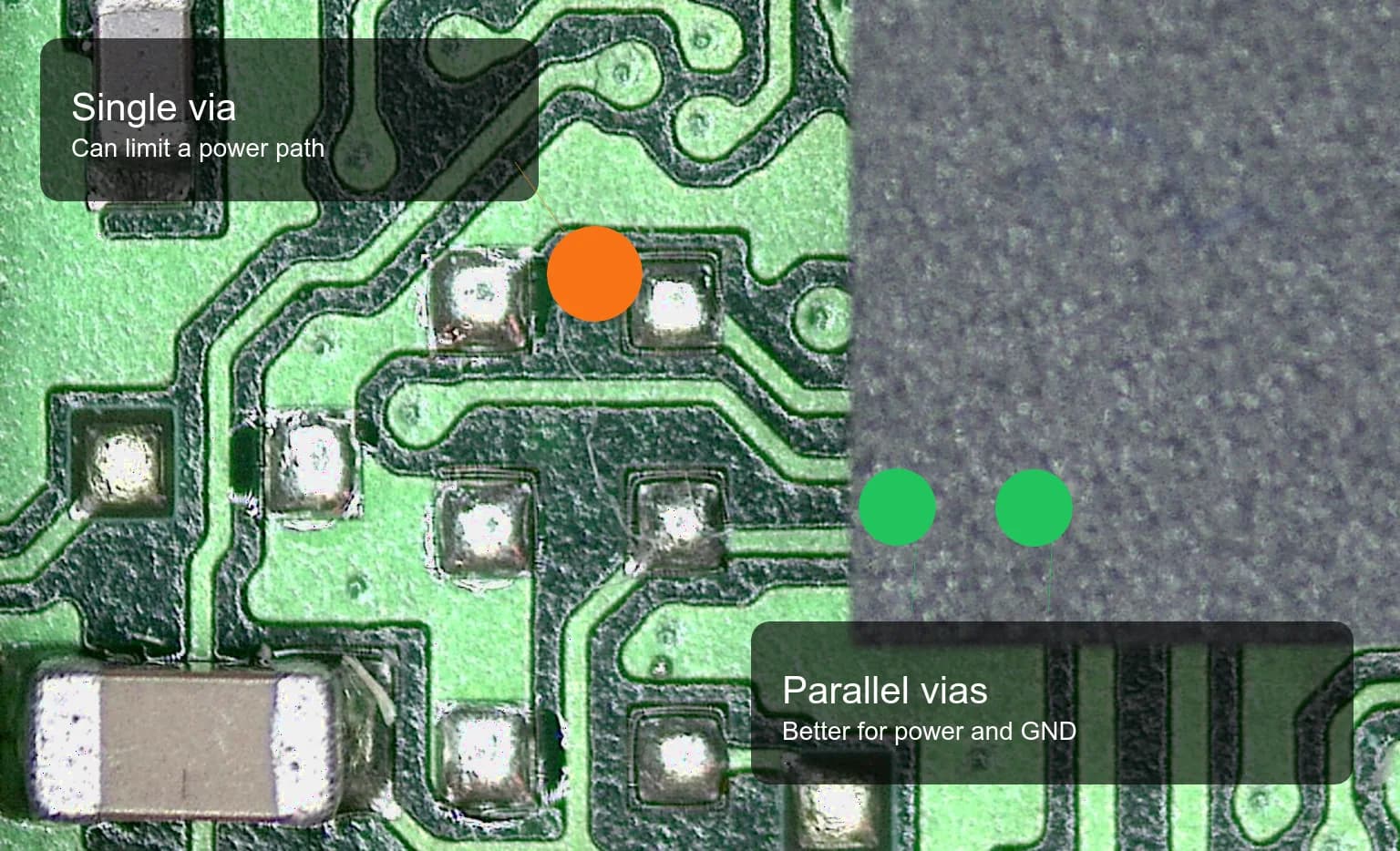
When power or ground changes layers, several vias in parallel are usually better than forcing all current through one small via.
Setting Up Net Classes in EasyEDA Pro or KiCad
Whether you use EasyEDA Pro, KiCad, or another PCB tool, it helps to create a few net classes before routing. The names do not need to match mine exactly. What matters is that each group has a clear job.
A simple setup:
| Net class | Used for | Starting trace width |
|---|---|---|
Signal | GPIO, I2C, UART | 0.15-0.20 mm |
Display_SPI | Display SPI routes | 0.20-0.30 mm |
Power_3V3 | Main 3.3V rail | 0.40-0.80 mm |
Power_5V | USB 5V, VBUS | 0.60-1.00 mm |
Battery | VBAT, BAT+ | 0.60-1.00 mm or more |
USB | D+ and D- | per USB routing rules, not current alone |
High_Current | Motors, LEDs, speakers, chargers | calculate from actual current |
USB is a good example of why net classes are not only about making traces wider. D+ and D- should be routed as a differential pair: close together, with consistent spacing, reasonable length matching, and away from noisy regions. That deserves its own rule set instead of being mixed into ordinary signals.
Common Power Routing Mistakes
These mistakes show up often on early PCB layouts:
- Using a narrow default trace for the main
3V3rail. - Letting the power path wander around the board because signal routing happened first.
- Placing decoupling capacitors correctly on the schematic but too far from the IC in layout.
- Using a single small via for an important power path.
- Splitting the ground plane with slots, keepouts, or routes so the return current has to detour.
- Running noisy power paths beside microphones, analog audio, antennas, or ADC traces.
- Forgetting to re-check net class assignments before exporting Gerbers.
These mistakes do not always kill a board immediately. More often, they create annoying intermittent problems: random resets, flickering displays, noisy audio, wrong sensor readings, or unreliable USB behavior.
A Quick Checklist Before Gerber Export
Before exporting Gerbers, I like to ask:
- Are the main power nets assigned to the correct net classes?
- Are
VBAT,5V, and3V3routed too narrowly anywhere? - Does any high-current path pass through one tiny via?
- If a power route changes layers, are there enough parallel vias?
- Is ground a useful plane, or has it been cut into isolated islands?
- Are decoupling capacitors close to the IC power pins?
- Does the main power route take an unnecessarily long path?
- Does DRC pass using rules that match the PCB manufacturer?
For small boards, doing these checks well already improves the layout a lot. You do not need to turn every trace into a highway. The point is to know which routes deserve priority: power, battery, high-current loads, ground return paths, and special signal pairs such as USB.
Conclusion
A net class is more than a settings panel in your PCB tool. It is a way to tell the tool what each route is supposed to be: a small logic signal, a board-level power path, a battery connection, or a special signal with its own routing rules.
When you are starting, keep the class setup simple, leave margin in trace width, and think about power before the board becomes crowded. A wider power trace, a more continuous ground plane, and a few well-placed parallel vias are small layout choices, but they can decide whether the prototype behaves calmly or turns into a long debugging session.
References
These sources are useful background material for checking terminology, limits, and engineering recommendations before applying the notes to a real prototype.
Share
Keep exploring
Read next
Related articles
PCB Ground Planes: GND Is More Than a Net Name
A practical guide to PCB ground planes, return current, GND layout mistakes, stitching vias, decoupling paths, and copper pour checks.
Choosing Capacitors for Electronics: Simple Part, Easy Mistake
A beginner guide to choosing capacitors for circuits: capacitance, voltage rating, decoupling, ceramic types, DC bias, and ESP32 values.
A Practical PCB Review Checklist Before You Send It to Fab
A practical PCB review checklist before fabrication: schematic, ERC, footprints, clearance, power, antenna, USB pairs, silkscreen, Gerbers, and BOM.