

A Practical PCB Review Checklist Before You Send It to Fab
A practical PCB review checklist before fabrication: schematic, ERC, footprints, clearance, power, antenna, USB pairs, silkscreen, Gerbers, and BOM.
Share
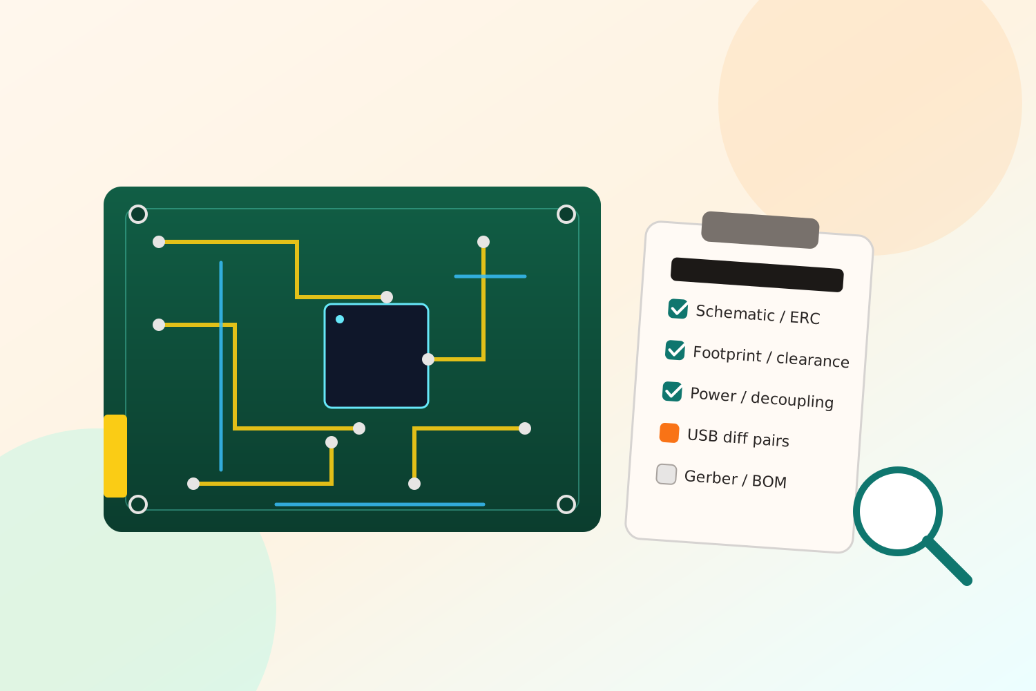
Sending a board to fab is easy. The button is right there. The expensive part is what happens after: a two-to-four week wait, then discovering a mirrored footprint, a missing ground pour, or a USB pair that was never length-matched. This checklist is the pass I actually run before clicking order, built around what tends to slip through: not typos, but assumptions that never got checked against the real schematic, the real footprint library, or the real fab's capabilities.
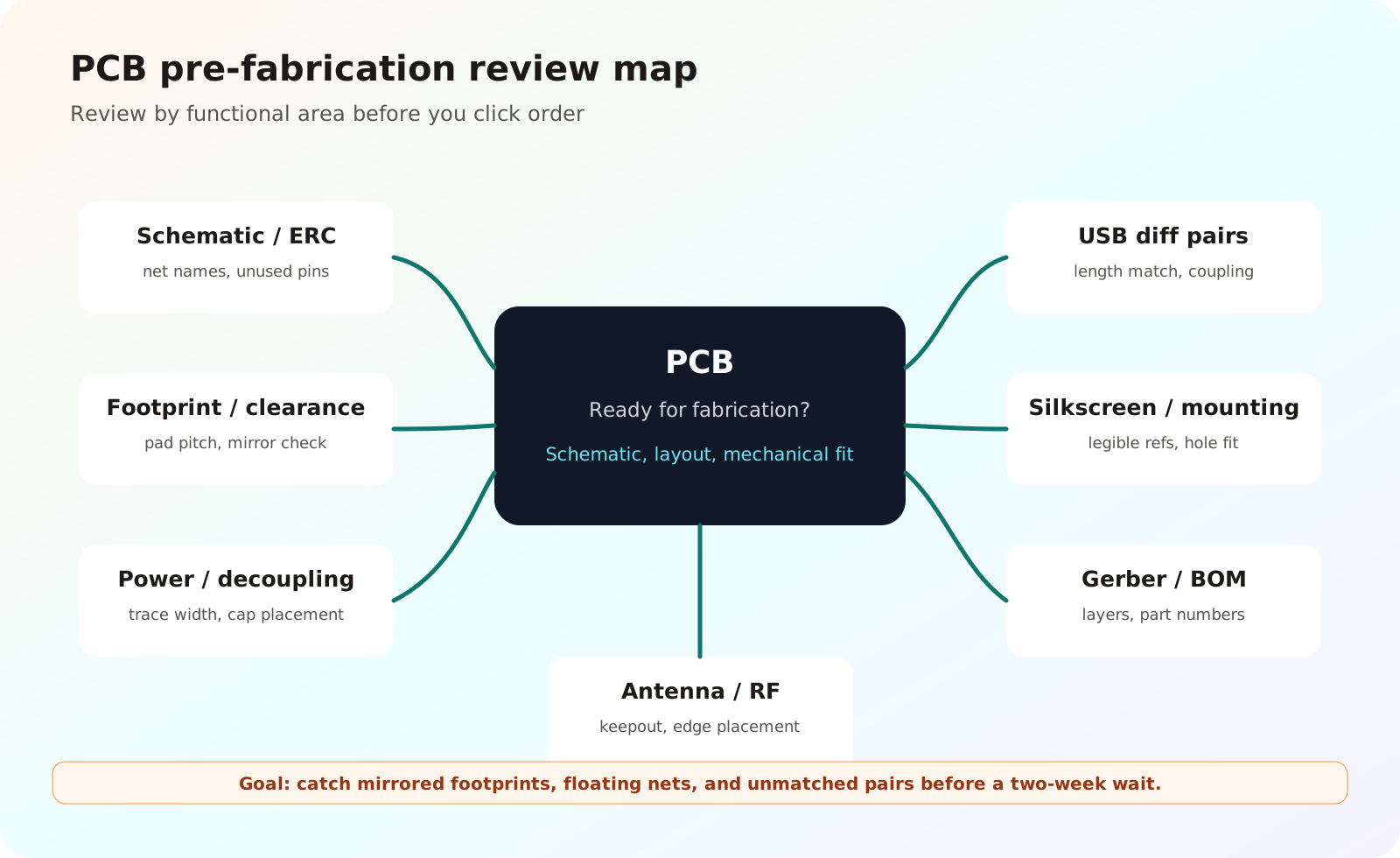
Review by functional area, not by scrolling the layout top to bottom.
Schematic and ERC First
A layout is only as trustworthy as the schematic behind it. Before touching the board view:
- Run the Electrical Rules Checker and read every warning, not just the errors. A "warning" about an unconnected pin is often a real bug wearing a soft label.
- Confirm every IC has its power and ground pins actually wired, not just present on the symbol. It is easy to place a decoupling capacitor near a pin that was never connected.
- Check that every net name that should be tied together really is —
GNDandAGND,3V3and3V3_MCU, are these meant to be the same net or intentionally separate? - Look for reference designator collisions or duplicates left over from copy-pasting a block.
- Confirm test points and unused pins are handled deliberately: pulled up/down as needed, or explicitly marked no-connect instead of left floating.
KiCad's ERC and DRC exist for exactly this pass — see the pcbnew documentation for what each rule actually checks before you assume "no errors" means "correct."
Footprints and Clearance
Footprint mistakes are the most common reason a board comes back unusable, because they are invisible until the part is in your hand.
- Verify every footprint against the part's real datasheet, not just the library default — pad pitch, pad size, and polarity marking (pin 1 dot, cathode band) especially for parts you sourced from a different footprint generator than usual.
- Check for mirrored footprints on connectors and asymmetric parts. A USB-C receptacle or a keyed connector placed backward is a classic, expensive mistake.
- Run the courtyard/clearance check and look at it visually, not just as a pass/fail count. Tall components near a connector or enclosure wall need real mechanical clearance, not just electrical clearance.
- Confirm your minimum trace width, spacing, and via size all sit safely inside your fab's stated capabilities — see JLCPCB's PCB capabilities for a concrete reference on trace/space, minimum drill, and annular ring if that is your fab.
- Double-check hole sizes for connectors and mechanical parts against the actual part, not a rounded guess.
Power
Power mistakes are the ones that turn "board doesn't work" into "board gets warm and stops working."
- Trace every rail from source to load and confirm decoupling capacitors sit close to the pins they serve, not just somewhere on the same net.
- Check current-carrying traces and pours are wide enough for the expected load, especially on any high-current path like a motor driver, LED array, or charging circuit.
- Confirm polarized components — electrolytic capacitors, diodes, some connectors — have their orientation correct in both schematic and footprint.
- Verify ground return paths are short and continuous, without a copper pour split cutting a return path in half by accident.
- If the board has multiple voltage domains, confirm there is no accidental short between them through a via, a silkscreen-only "keepout," or a missing split in a pour.
Antenna and RF
If the board has Wi-Fi, Bluetooth, LoRa, or any other RF section, this section is not optional, even on a "simple" board.
- Keep the keepout area under and around the antenna free of copper, silkscreen, and components, exactly as the module's reference design specifies.
- Confirm the antenna sits near a board edge with nothing metal — connectors, shields, batteries — close enough to detune it.
- Check impedance-controlled RF traces follow the module vendor's trace width and reference-plane guidance, not a generic trace width.
- If using a certified module, verify you have not modified the RF section in a way that voids that certification.
USB Differential Pairs
USB signal integrity problems rarely show up as "doesn't work at all" — they show up as flaky enumeration, random disconnects, or a device that only works on some hosts.
- Confirm D+ and D- are routed as a matched differential pair: tightly coupled, consistent spacing, and length-matched to within your controller's tolerance.
- Avoid routing the pair through vias unnecessarily, and keep any unavoidable vias matched on both traces.
- Check the pair does not run parallel to a noisy signal (a switching regulator's switch node, a clock line) for any significant length.
- Confirm ESD protection sits close to the connector, on the connector side of anything sensitive.
Silkscreen and Mounting
These feel cosmetic until the board is in an enclosure or in someone else's hands.
- Confirm reference designators are legible, not hidden under a component, and consistent with the schematic — this matters as much for future-you debugging as for anyone else.
- Check polarity and orientation markings (pin 1, connector keying, LED polarity) are visible after assembly, not tucked under the part itself.
- Verify mounting hole sizes, positions, and keepout match the enclosure or standoff hardware you are actually using, not a placeholder from a template.
- Confirm silkscreen text meets your fab's minimum size and line width — text that reads fine on screen can disappear at real print resolution.
Gerbers and BOM: the Last Pass
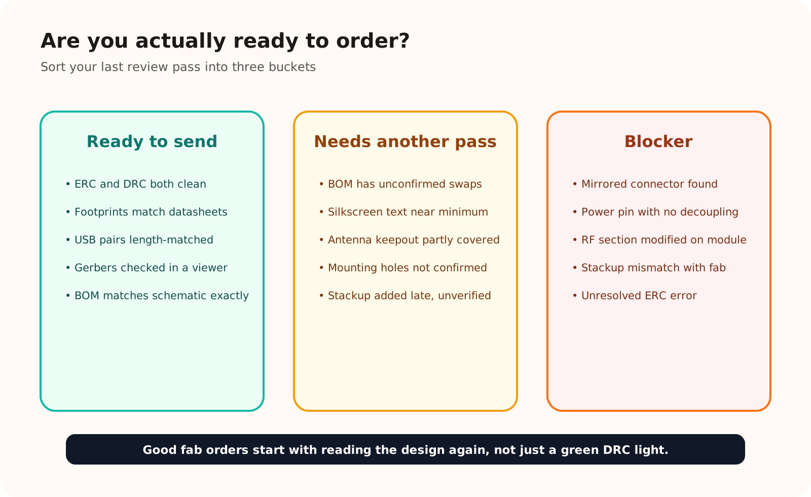
Sort your last review pass into these three buckets before you order.
Before uploading anything, treat this as a separate pass from layout review, because export mistakes are different from design mistakes.
- Open the generated Gerbers and drill files in a separate viewer (not just your CAD tool's own preview) and check every layer is present: copper layers, solder mask, silkscreen, paste, and the correct outline/edge-cuts layer.
- Confirm layer count and stackup match what you configured with the fab, especially after any late-stage layer additions.
- Check the BOM references match your schematic exactly — designator, value, footprint, and manufacturer part number — and that nothing was auto-substituted to an out-of-stock alternative without your review.
- Confirm your fab's specific requirements (panel size, tooling holes, min silkscreen size, impedance control if used) are met — check the current numbers on your fab's own capabilities page, since they do change.
- Do one final side-by-side: layout view, schematic, and BOM open together, checking that what you are about to pay for is actually what you designed.
Conclusion
None of these checks are exotic. Each one is a place where a real board has come back wrong before — a mirrored footprint, a floating pin marked "fine" by ERC's silence, a USB pair that was never actually matched. Running through this list deliberately, instead of trusting that "no errors" in one tool means the board is ready, is what turns a fab order into a board that works the first time.
References
Related reading
Share
Keep exploring
Read next
Related articles
Net Classes and Trace Width: When Should a PCB Trace Be Wider?
A practical guide to PCB net classes and trace width for small boards: signal traces, 3V3, 5V, battery paths, ground, power vias, and a pre-Gerber checklist.
PCB Ground Planes: GND Is More Than a Net Name
A practical guide to PCB ground planes, return current, GND layout mistakes, stitching vias, decoupling paths, and copper pour checks.
GPT-6 Astra and the Future of PCB Design: Speed Up or Replace Engineers?
How far can GPT-6 Astra go in KiCad? An independent look at the demo, EEBench, open-source tools, and why routing a board is not the same as making it production-ready.