

EJA M v1.0 - ESP32 LoRa/GPS Board for a Marine Monitoring Buoy
Author: Leonardo Ward
Open-source PCB design for EJA M v1.0, an ESP32-WROOM-32D board with LoRa, GPS, an RTC, and battery/servo power management, built for an ocean monitoring buoy.
Main components
Share
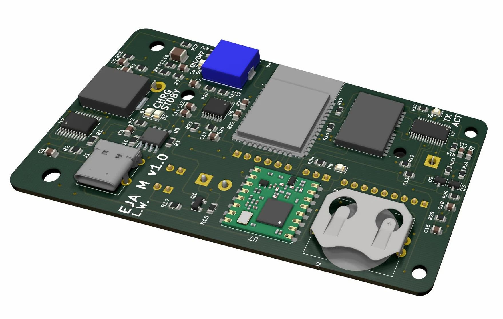
PCB photos
Quick Specs
- Main IC
- ESP32-WROOM-32D (4MB)
- Status
- Concept
What it is
An open-source ESP32 board built for an ocean monitoring buoy, combining long-range LoRa telemetry, GPS positioning, real-time clock scheduling, a battery charging/regulation chain, and a servo motor driver on one PCB. It's the third iteration of the author's buoy electronics, replacing two earlier separate boards (Buoy A and Buoy B) and an onboard gateway design with a single consolidated board.
Main components
- ESP32-WROOM-32D (4MB), the main microcontroller
- RFM95W-915S2 LoRa transceiver with a U.FL antenna connector
- ATGM332D-5N31 GPS module with a U.FL antenna connector and CR2032 backup cell
- DS3231M real-time clock
- FT260S-U USB-to-UART/I2C bridge with an auto-reset circuit for the ESP32
- TP4056 Li-Ion charger for an 18650 cell, with charge/standby LEDs
- LTC3113 SEPIC converter (steady 3.3V regardless of battery charge state)
- TPS61030 boost converter (5V/2A) for an external servo motor
- LTC2954 pushbutton on/off controller
- ADXL343 accelerometer connector, plus a header for unused ESP32 pins
What you can use it for
- Building the EJA ocean monitoring buoy electronics as designed
- Any battery-powered ESP32 project that needs LoRa + GPS + RTC + a regulated servo rail on one board
- A reference design for USB-C EMC protection, an FTDI-based auto-reset circuit, and battery-voltage-independent 3.3V regulation via SEPIC
Notes before use
- Nastrotek has not independently fabricated or tested this board yet.
- This is an upgrade/replacement of the author's earlier Buoy A, Buoy B, and Onboard Gateway designs, developed as part of the "EJA" project for the Hackaday 2021 Dream Team.
- Do not solder both R32 and R33 — they're alternate jumpers (SEPIC output vs. direct battery) and soldering both shorts 3.3V to the battery rail. The author's own notes say plainly: do not solder R33.
- PCB dimensions (97.5 x 51.2mm) and a keep-out region on the back layer are dictated by the buoy enclosure — check
pcb_dimensions_boundaries.pngbefore reusing the outline for a different enclosure. - Licensed under the Apache License 2.0.
Source / reference
Original hardware design by Leonardo Ward, part of the EJA project on Hackaday.io.
The PCB images on this page are retained from the source repository and attributed to Leonardo Ward under the Apache License 2.0. Nastrotek does not claim ownership of the original design or images.
How to evaluate this board
Read this resource as a starting point for review, not as a board you should manufacture blindly. Open the schematic first and identify the power input, regulator path, MCU or main controller, external connectors, programming interface, and any sensor or display interfaces. Once the functional blocks are clear, it becomes much easier to decide whether the design matches your project.
For a buoy board, I would review the harsh-environment details before anything cosmetic: power input protection, LoRa/GPS antenna routing, connector sealing, corrosion risk, test points for field repair, and whether the ESP32 can still be flashed after the board is potted or mounted. The layout has to serve maintenance, not just pass DRC.
Before reusing the files
- Check the license and original author notes.
- Confirm voltage levels before connecting external modules.
- Verify connector pinout against your cables and sensors.
- Review BOM availability before ordering PCBs.
- Export fresh Gerbers from the design tool if you modify anything.
- Treat untested designs as references until you have fabricated and measured them.
Good use cases
This kind of resource is useful when you want to study a real open-source hardware design, borrow part of a circuit, or compare layout decisions before creating your own board. Even if you do not fabricate the PCB directly, the schematic can still be valuable as a reference for power design, connector planning, enclosure constraints, or firmware bring-up.
For a small product prototype, the best workflow is to reuse ideas carefully: copy the principle, not the entire board without context. Mark what you changed, keep notes on assumptions, and add measurement points so the first fabricated board can teach you something useful.
Related reading
Download Resource
File details & download
- File type
- Design File
- Version
- v1.0
- File size
- Not specified
- Author
- Leonardo Ward
- Original source
- Open original source · github.com
- License
- Not verified
- Commercial use
- Not verified
- Last checked / updated
- Jul 31, 2026
- Tested by Nastrotek
- Not verified
The license has not been verified. Do not assume this resource is free to reuse, redistribute, or use commercially.
Share
Keep exploring
Read next
Related articles
GPT-6 Astra and the Future of PCB Design: Speed Up or Replace Engineers?
How far can GPT-6 Astra go in KiCad? An independent look at the demo, EEBench, open-source tools, and why routing a board is not the same as making it production-ready.
Net Classes and Trace Width: When Should a PCB Trace Be Wider?
A practical guide to PCB net classes and trace width for small boards: signal traces, 3V3, 5V, battery paths, ground, power vias, and a pre-Gerber checklist.
PCB Ground Planes: GND Is More Than a Net Name
A practical guide to PCB ground planes, return current, GND layout mistakes, stitching vias, decoupling paths, and copper pour checks.