

ESP32 Battery Power Design: From USB-C Charging to the 3.3V Rail
Review an ESP32-S3 battery power path from USB-C and TP4056 charging to protection, load sharing, 3.3V regulation, and load budget.
Share
I use the checks below to help you turn a battery-powered ESP32 idea into a design with realistic runtime and fewer power surprises.
An ESP32 board can behave perfectly on a USB bench supply and fail the moment you move it to a battery. Add a display, microphone, and speaker, and the supply has to solve several problems at once: accept 5V from USB-C, charge a single Li-ion cell safely, prevent backfeed, protect the cell, generate a clean 3.3V rail, and survive Wi-Fi and audio load steps.
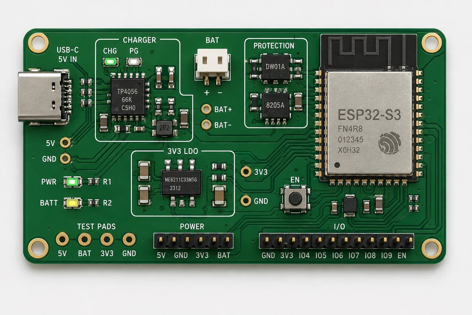
The circuit in this article uses components such as: USB-C power-only, TP4056, single-cell battery connector, DW01A + 8205A pair, MOSFET AO3407A, LDO ME6211C33M5G, and test pads for 5V, BAT, 3V3, and GND.
Start with the whole energy path
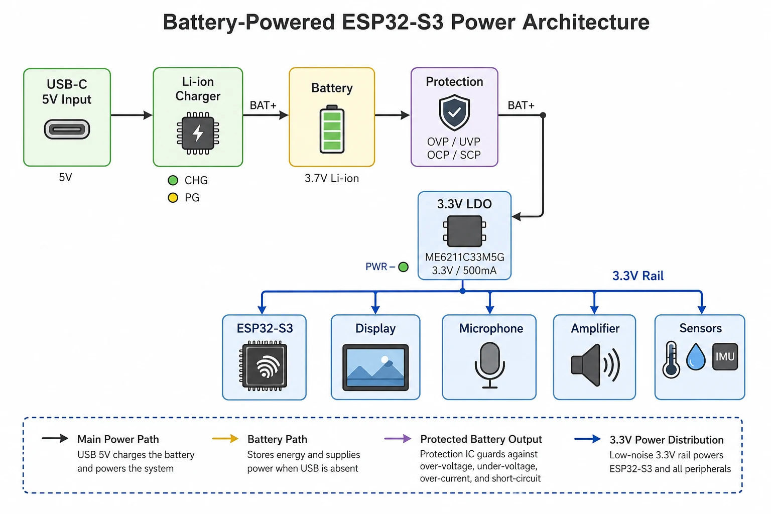
The board-level overview is useful, but the power-path still needs schematic-level verification.
The illustrated architecture is:
USB-C 5V → charger → 1S cell → protection → 3.3V regulator → loads
Those loads include the ESP32-S3, display, microphone, amplifier, and sensors. This is a sensible first decomposition, but it leaves two critical questions unanswered:
- What powers the system when USB and the battery are both present?
- Can a 3.3V rail remain regulated while the cell falls from 4.2V toward 3.0V?
The answers determine the power-path and regulator topology. A board can light its status LED on the bench and still reset when Wi-Fi transmits, volume rises, or the USB cable is removed.
Power-only USB-C still needs correct CC wiring
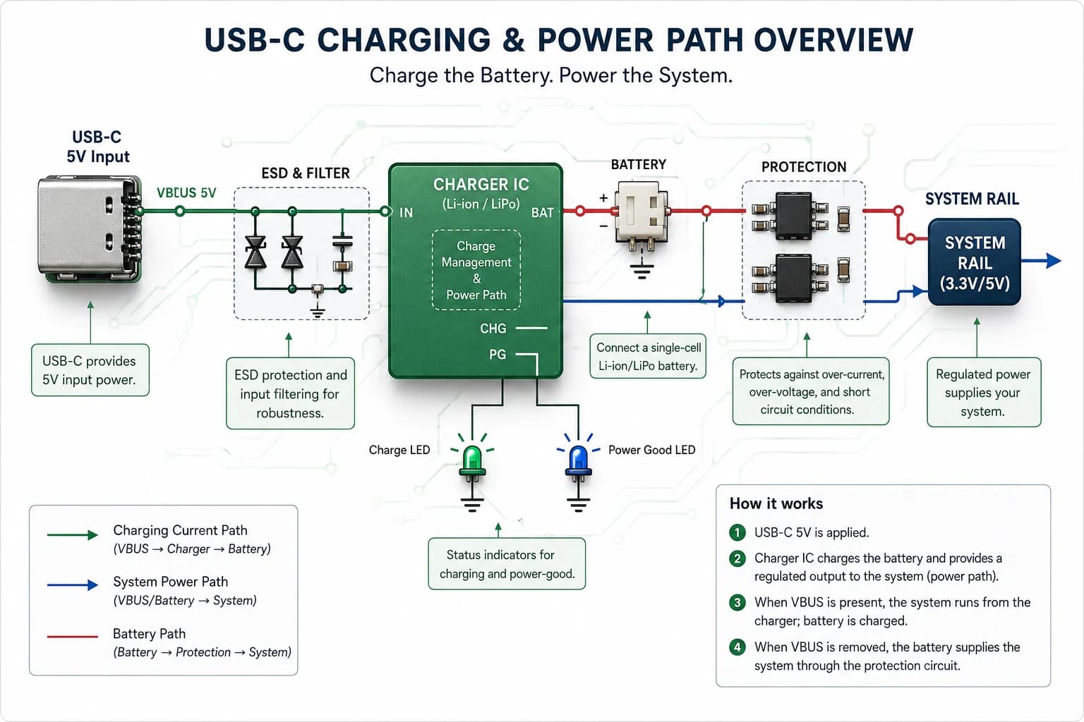
Charging the cell and powering the load are related but distinct design problems.
The case-study schematic leaves D+ and D- unconnected, so the Type-C receptacle is used for power only. Both CC1 and CC2 have independent 5.1kΩ pull-down resistors to ground, identifying the board as a sink regardless of plug orientation.
This design needs only the default 5V supply and does not require USB Power Delivery negotiation. That does not mean every USB-C source can be treated as an unlimited 5V supply. If the product needs more current than the source advertises, or needs a higher voltage such as 9V or 12V, it must detect the Type-C current advertisement or use an appropriate PD controller.
The input network shown in the schematic includes:
L1, marked 600Ω at 100MHz, as a high-frequency ferrite bead.C1 = 10µFfor bulk support andC2 = 100nFfor faster transients.- An
SMF5.0ATVS on VBUS. - A grounded connector shield.
This is a useful starting point, but the TVS must be selected for working voltage, capacitance, and the surge environment. Place ESD protection near the connector, make its return path short, and keep discharge current away from the ESP32-S3 RF area and sensitive ground returns.
Choose charge current from the cell backward
The charger block uses a TP4056 with a 2kΩ programming resistor. Depending on the exact TP4056 vendor and datasheet revision, that value commonly produces a nominal charge current around 0.5–0.58A. The final setting should not be chosen simply because the IC supports it. It must respect the smallest of four limits:
Icharge ≤ min(
  cell charge-current rating,
  USB input budget minus system load,
  charger and PCB thermal limit,
  connector and protection-path rating
)
The TP4056 is a linear charger. With a cell at 3.2V and 0.5A charge current, its approximate dissipation is:
Pcharger ≈ (5.0V - 3.2V) × 0.5A = 0.9W
That is substantial heat in a small package. Thermal regulation may reduce the actual current below the resistor-programmed value when copper area or airflow is insufficient. Validate the charger with a depleted cell, the highest expected USB input, and the worst ambient temperature.
The CHG and STBY/PG LEDs are convenient during bring-up, but they consume current too. A low-power product should include them in the sleep budget or make them optional placements.
A charger is not automatically a power-path controller
The overview image shows the charger supplying the system while it charges the battery. That is desirable behavior, but a TP4056 is fundamentally a single-cell charger. It does not expose a dedicated system output with managed load sharing like a purpose-built power-path PMIC.
In the case-study schematic, BAT_OUT, 5V, and the VBAT node meet around Q2, an AO3407A P-channel MOSFET, before the LDO. The apparent intent is automatic source selection with reduced backfeed. Before reusing this circuit, verify:
- Q2 source, drain, and body-diode orientation in both USB-present and USB-absent modes.
- Whether 5V can feed backward into the cell, protection stage, or charger BAT pin.
- Whether system current prevents battery current from falling below the termination threshold.
- How far
VBATand3V3dip when USB is inserted or removed. - Whether input current and charger dissipation remain acceptable while charging and running together.
A true power-path normally gives the load priority from USB, directs the remaining current to the cell, and changes to battery power without a disruptive rail drop. For products that routinely operate while charging, an integrated load-sharing charger is generally easier to validate than a custom MOSFET arrangement.
| Operating mode | Intended load source | What to measure |
|---|---|---|
| USB only, no cell | USB → system rail | Rail behavior and charger state without a battery |
| Battery only | Protected cell → regulator | Dropout, brownout, and sleep current |
| USB plus charging cell | USB serves load first; remainder charges cell | VBUS current, cell current, charger temperature |
| USB removed under load | Battery takes over | Rail droop and ESP32 reset behavior |
| Full cell with active load | USB serves load | Correct charge termination and recharge behavior |
Cell protection is not complete battery management
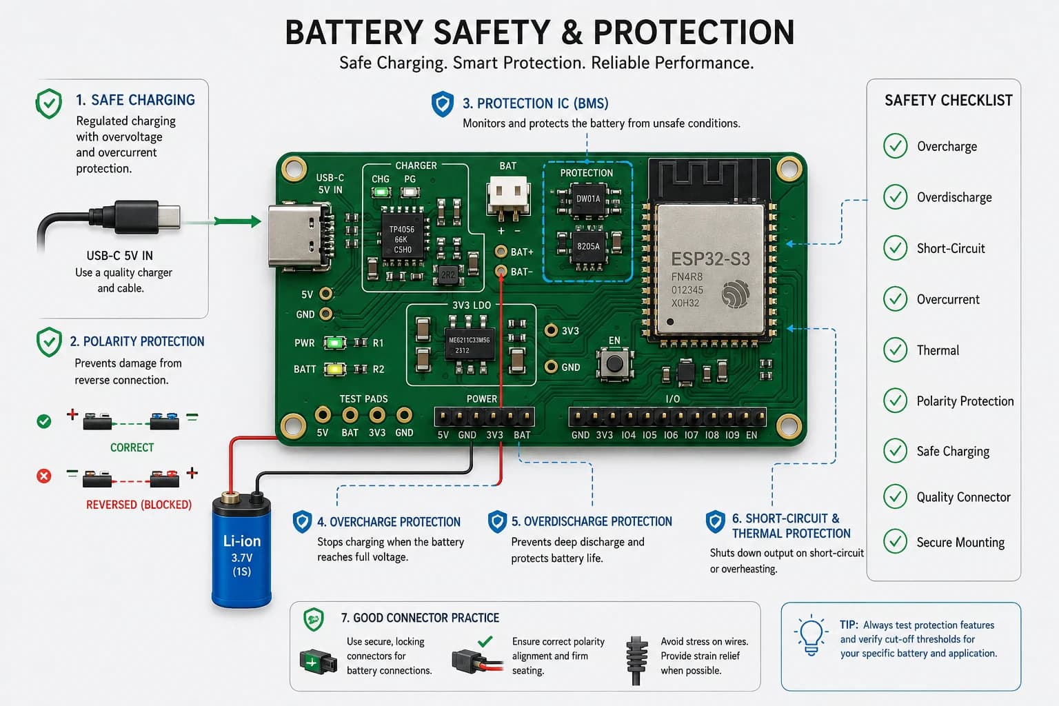
Treat the pictured checklist as system goals and verify which functions the selected parts actually implement.
The board uses a DW01A and dual 8205A MOSFETs. This familiar combination normally disconnects the cell for overcharge, over-discharge, over-current, and short-circuit conditions. It is the last protection layer, not the charge algorithm, and it should not become the product's routine shutdown mechanism.
The safety illustration also lists thermal and reverse-polarity protection. Read those as system requirements, not functions automatically provided by the DW01A and 8205A:
- The DW01A does not sense cell temperature. Battery thermal protection needs an NTC and a charger or BMS input that actually evaluates it. Confirm whether the TP4056
TEMPpin in the final schematic uses a sensor or is disabled. - Reverse-polarity behavior depends on the connector and MOSFET topology. A two-pin JST-style connector does not prevent a supplier from wiring a pack with opposite polarity.
- OVP, UVP, and OCP thresholds vary by exact part and vendor. Read the purchased component's datasheet and measure the trip points on hardware.
- The protection MOSFETs carry both charge and load current, so
BAT-andBAT_OUTpaths need short, wide copper and deliberate returns.
Firmware should monitor battery voltage and shut down gracefully before the protection IC opens the cell. That protects storage, avoids speaker pops, and gives the UI time to show a low-battery state.
A 500mA LDO does not leave 500mA for the whole product
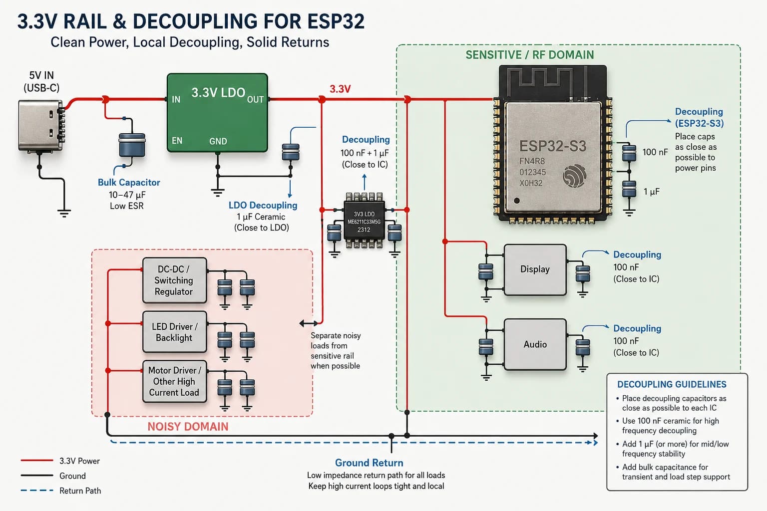
Correct capacitor values cannot compensate for poor placement at fast load transients.
U3 is shown as an ME6211C33M5G 3.3V LDO rated at 500mA. Espressif recommends a 3.3V supply capable of at least 500mA for the ESP32-S3 itself. If the same regulator also powers the display, microphone, amplifier, and sensors, the paper design has already consumed its current margin before peak behavior is considered.
A 1S Li-ion cell spans roughly 4.2V when full to around 3.0V near depletion. A 3.3V LDO regulates only while:
Vbattery > 3.3V + Vdropout
Below that point, the output follows the battery minus internal losses. ESP32-S3 main supply rails are specified for 3.0–3.6V operation, so the system may brown out before the battery protection reaches its over-discharge threshold. That can be an intentional early cutoff, but it reduces usable capacity compared with a simple mAh estimate.
There are three common approaches:
- Keep the LDO for a modest load, accept unused capacity near the end of discharge, and verify clean brownout behavior.
- Move the amplifier or display backlight to another rail so the sensitive 3.3V supply serves only the ESP32 and low-current logic.
- Use a 3.3V buck-boost converter when most of the 4.2–3.0V cell range must remain usable.
Avoid placing a high-power speaker load directly on the sensitive rail without analysis. Audio amplifiers, motors, and PWM backlights need local energy storage, adequate copper, and return paths that do not share a narrow segment with ESP32 RF or analog ground.
Capacitor value is only half the design
The schematic places C4 10µF + C5 100nF at the LDO input and C6 10µF + C7 100nF at its output. Near the ESP32-S3 module, C9 10µF is accompanied by C10–C14 100nF. This bulk-plus-local-decoupling pattern aligns with Espressif's guidance: at least 10µF at the power entrance, 0.1µF close to digital supply pins, and additional support on the analog rail for RF current steps.
During layout:
- Place each 100nF capacitor at its target supply pin with the smallest practical
VDD → capacitor → GNDloop. - Put 10µF near the rail entrance and near the ESP32-S3 cluster when those locations are physically separated.
- Maintain an uninterrupted ground plane beneath the module and regulator.
- Do not connect a capacitor through a long, thin branch before returning to the IC.
- Check the selected LDO's ESR and capacitance stability requirements; ceramic capacitors lose effective capacitance under DC bias.
Bulk capacitance supports slower load changes, while 100nF capacitors handle faster edges. A large number of poorly placed capacitors is less effective than a smaller, deliberate network.
Budget Wi-Fi, display, and audio together
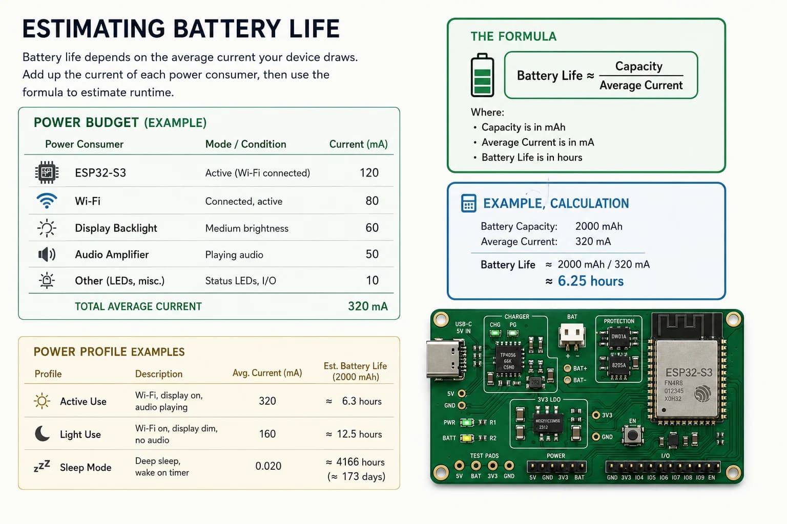
The 6.25-hour result is idealized and excludes conversion loss, usable-capacity margin, and peak loads.
The supplied budget uses these example averages:
| Load | Current in the illustration |
|---|---|
| Active ESP32-S3 | 120mA |
| Active Wi-Fi | 80mA |
| Medium display backlight | 60mA |
| Audio amplifier | 50mA |
| LEDs and miscellaneous | 10mA |
| Total | 320mA |
For a 2,000mAh battery, the ideal calculation is 2000 / 320 = 6.25 hours. That is useful as an order-of-magnitude check, not as a runtime specification.
First determine whether the 120mA ESP32-S3 measurement already includes the Wi-Fi radio. If it represents the complete module while connected, adding another 80mA counts Wi-Fi twice. The reliable method is to measure complete product modes at the battery input: idle, listening, Wi-Fi transmit, display active, talking, and deep sleep.
Then account for usable capacity and operating conditions:
Runtime ≈ rated_capacity × usable_fraction × aging_factor
          / average_battery_current
With a usable fraction around 0.75–0.9 depending on cutoff, load, and temperature, the ideal 6.25 hours may become roughly 4.7–5.6 hours before aging. This is still an estimate; the final number comes from a discharge test using the selected cell.
Peak current matters as much as average current. A Wi-Fi transmit burst can overlap an audio transient for a few milliseconds. A 500mA LDO near its limit may dip even when a multimeter reports only a 320mA average. Probe 3V3 at the module with an oscilloscope and trigger around radio transmission or playback start.
Charging while running also changes the arithmetic. If USB provides 500mA and the system consumes 320mA, the battery cannot simultaneously receive 500mA. Before loss and thermal limiting, only about 180mA remains. Without a true power-path, current allocation and charge termination become even less predictable.
Read the case-study schematic by following energy
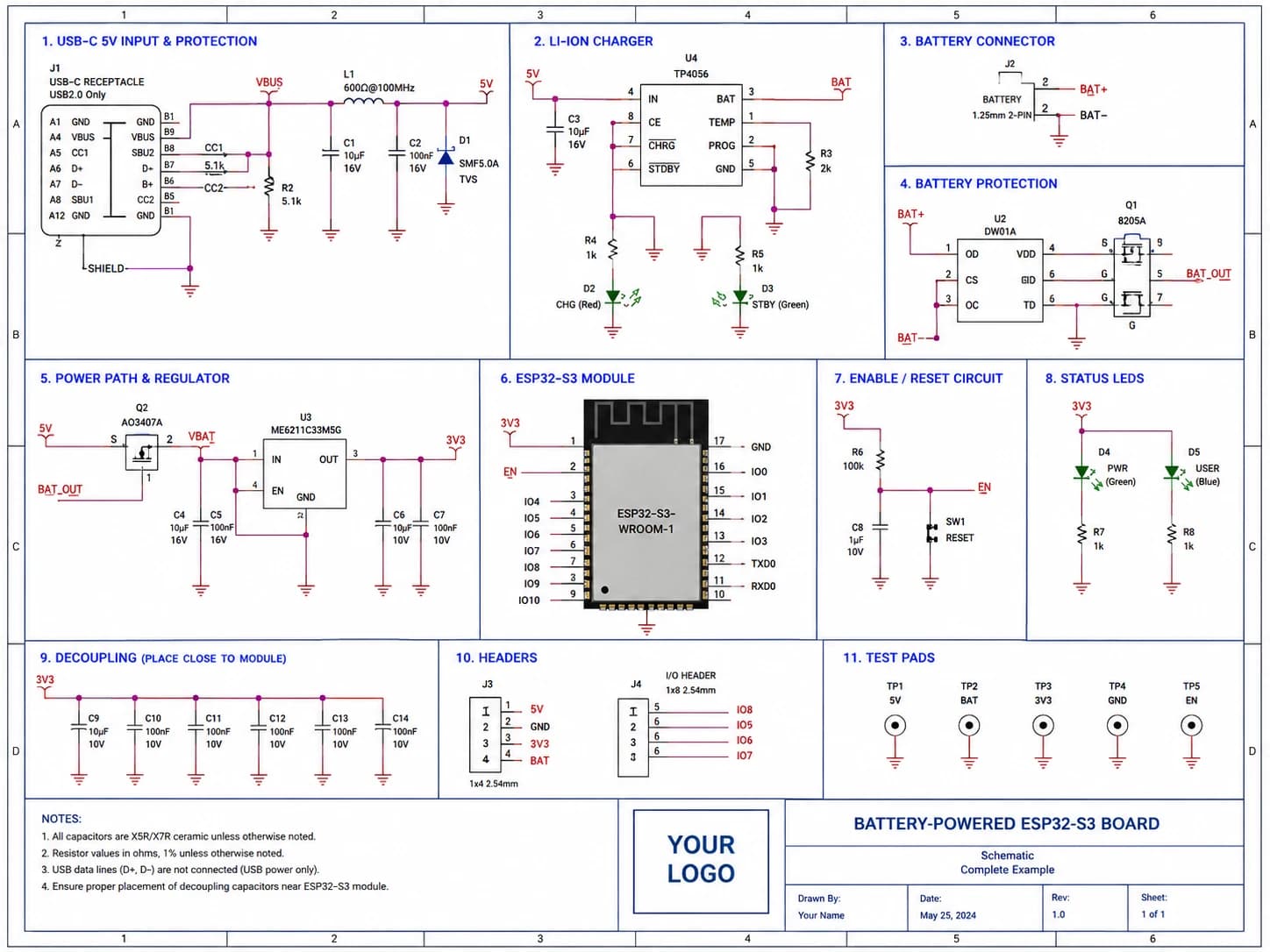
The case-study schematic is split into 11 blocks for power, protection, reset, decoupling, and test-point review.
The schematic is organized into 11 blocks. Review them by following energy flow rather than component numbering:
- USB-C input: 5.1kΩ CC resistors, ferrite, TVS, and input capacitors.
- Charger: TP4056, programming resistor, charge/standby LEDs, and TEMP handling.
- Battery connector: polarity, pitch, current rating, and mechanical retention.
- Protection: DW01A plus 8205A, trip thresholds, and high-current paths.
- Power path/regulator: AO3407A,
VBAT, ME6211 3.3V output, and backfeed behavior. - ESP32-S3 module: all required rails must rise together and remain within range.
- EN/reset: the drawing uses R6 = 100kΩ and C8 = 1µF; compare its timing with the exact module guidance.
- Status LEDs: include their current in the sleep budget or make them optional.
- Decoupling: verify physical placement, not only schematic values.
- Headers: prevent accidental shorts among
5V,BAT, and3V3. - Test pads:
5V,BAT,3V3,GND, andENare a practical bring-up minimum.
The image is a complete schematic presentation, not evidence that the board has passed electrical validation. Before reuse, simulate or measure each supply mode, verify every package pinout, and consult the datasheet for the exact parts being purchased.
Turn the schematic into a measurable PCB
This is a reference-board render, not a photograph of a fabricated PCB; the silkscreen is organized for bring-up.
The top view separates USB-C, charger, BAT, protection, 3V3 LDO, and ESP32-S3 with clear silkscreen. Test pads sit at the board edge, which is useful when several rails must be observed at once. This is a productive prototype layout convention because power faults rarely yield to a single measurement.
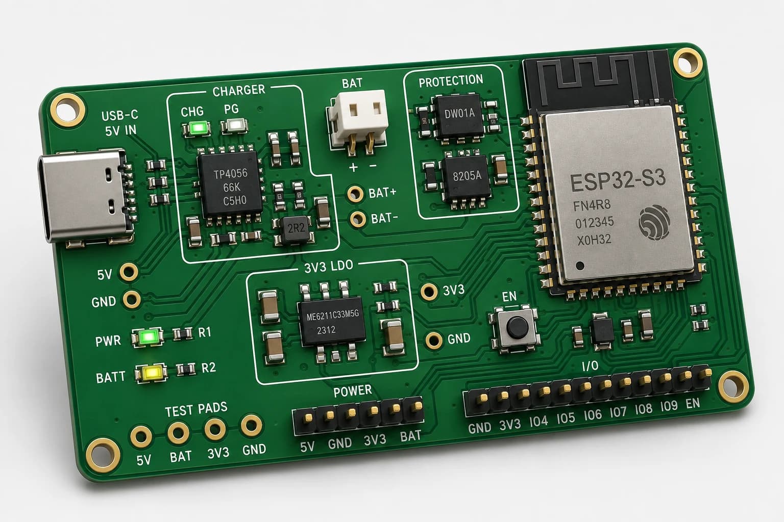
On the real layout, high-current paths and return loops matter more than spacing suggested by the render.
The perspective render communicates placement but cannot reveal copper width via stitching, ground layers, or thermal-pad implementation. On the real board, prioritize:
- Wide enough VBUS, BAT, BAT_OUT, and 3V3 paths for peak current.
- Charger copper area that meets the package's thermal guidance.
- Protection MOSFETs close to the cell connector with a compact current loop.
- A tight LDO cluster with its input and output capacitors.
- The ESP32-S3 antenna keepout free from copper, the cell, and power wiring.
- An amplifier return that does not share a narrow ground segment with the ESP32.
Once a physical PCB exists, USB-C present with the Li-ion cell attached is the operating mode that deserves the longest validation run because the source, charger, load, and cell all interact. At minimum, log VBUS, VBAT, 3V3, USB input current, cell current, and TP4056 temperature with a depleted cell, a nearly full cell, and simultaneous Wi-Fi plus audio activity.
Pre-layout checklist
- Confirm the cell chemistry, charge profile, and maximum charge current from its datasheet.
- Verify USB-C sink resistors and never assume a PD current budget without negotiation.
- Review MOSFET orientation, body diodes, and every possible backfeed route.
- Measure or simulate source switchover during USB insertion and removal.
- Size the LDO or buck-boost for peak current, dropout, thermal behavior, and capacitor stability.
- Separate noisy loads from sensitive rails where necessary and design return paths deliberately.
- Let firmware shut down before the protection IC's hard cutoff.
- Provide test points for 5V, battery, system rail, 3.3V, ground, and EN.
- Test short circuit, reversed pack, hot plug, and thermal behavior under controlled conditions.
- Never treat a render or illustrative schematic as a replacement for prototype validation.
Conclusion
An ESP32-S3 battery supply is not finished when a charger and LDO have been selected. USB-C, the cell, protection, power-path, regulator, capacitors, and PCB layout must be reviewed as one system. This case-study board gives us a clear map, while highlighting the measurements that still matter: real charge current, TP4056 temperature, 3.3V dropout, backfeed, and peak load with Wi-Fi, display, and audio operating together.
For a larger robot design, continue with the ESP32-S3 Mochi hardware architecture and full-duplex ESP32-S3 I2S audio design to connect the power budget to real peripheral loads.
References
Share
Keep exploring
Read next
Related articles
What Is a MEMS Microphone? From a Silicon Diaphragm to ESP32 Audio
Learn how MEMS microphones work, how analog, PDM, and I2S outputs differ, and how to avoid PCB, power, and acoustic-port mistakes.
Complete Hardware Architecture for an ESP32-S3 Mochi Robot
A practical breakdown of ESP32-S3 Mochi Robot hardware: display, touch, I2S microphone, amplifier, speaker, battery, charging, and GPIO.
ESP32-C3 or ESP32-S3: Which Chip for a Robot with a Screen and Audio?
Comparing ESP32-C3 and ESP32-S3 on GPIO, RAM, PSRAM, USB, I2S, and LVGL headroom, with a concrete recommendation for a basic Mochi build and a Mochi AI build.